

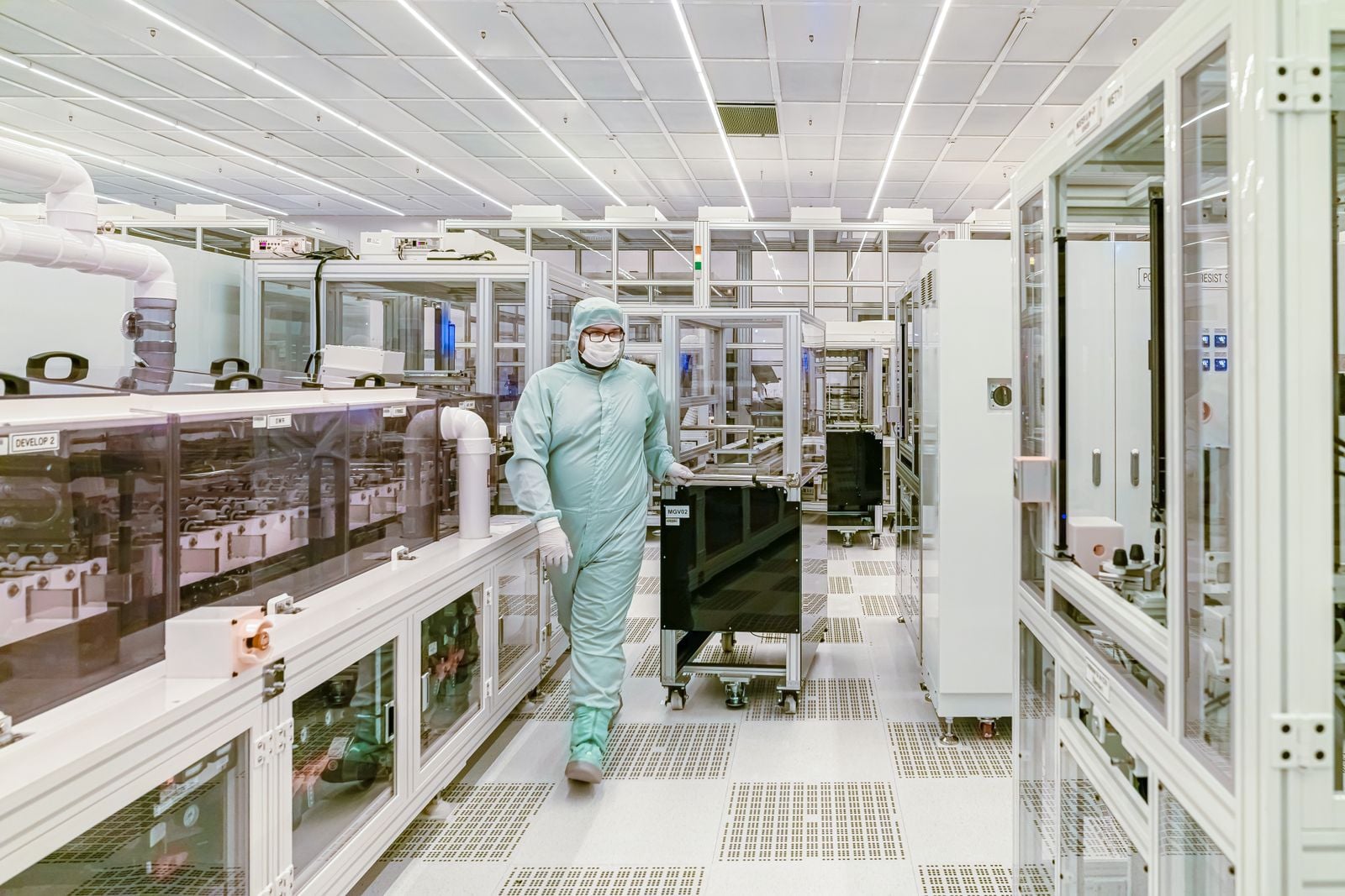
Inside a cleanroom in Veldhoven, a town of 45,000 people in the southern Netherlands, technicians are assembling a machine that no other company on Earth knows how to build. It stands roughly the height of a double-decker bus, weighs about 180 tonnes, costs upwards of $400 million in its newest configuration, and contains a set of mirrors polished to a smoothness so extreme that if one were scaled up to cover the surface area of Germany — 357,000 square kilometres — its tallest imperfection would rise less than a millimetre off the ground.
The machine is an extreme ultraviolet lithography system. The company is ASML. Every advanced processor shipped in an iPhone, every Nvidia AI accelerator sitting in a hyperscaler’s data centre, every leading-edge chip Intel, TSMC or Samsung has made in the last five years has passed under the light of one of these machines.
There are no competitors. Not one.
What the mirrors actually do
EUV lithography prints the patterns that become transistors. The wavelength of light used — 13.5 nanometres — is so short that no lens material on Earth can focus it. Glass absorbs it. Air absorbs it. The entire optical path has to run through a vacuum, and the light has to bounce off mirrors rather than pass through lenses.
Those mirrors are the technical heart of the machine. They are manufactured by Zeiss SMT in Oberkochen, Germany, from ultra-low-expansion glass, coated with alternating layers of molybdenum and silicon just a few atoms thick, and polished to a surface roughness measured in picometres — trillionths of a metre. The Germany-scaled-to-a-millimetre comparison is the standard way Zeiss and ASML describe the tolerance, and it holds up: the mirrors are smoother than anything that has ever been mass-produced.
To generate the EUV light itself, droplets of molten tin roughly 25 micrometres across — smaller than a human hair is thick — are fired into the vacuum chamber at 70 metres per second. A pulsed laser hits each droplet twice. The second pulse vaporises it into a plasma at around 220,000 degrees Celsius, which radiates in the 13.5 nm band. This happens 50,000 times a second. The plasma light is collected by a curved mirror, bounced through the optical column, reflected off the patterned mask, and finally focused onto the silicon wafer.
The scale of the manufacturing feat
The engineering underneath that mirror specification sits at the frontier of what physics allows. A recent review published in Materials Futures by Lifei Zhang and Xinchun Lu at Tsinghua University describes the shift toward atomic-scale chemical mechanical polishing as the semiconductor industry pushes past Moore’s Law. The authors describe the coupling of chemical reactions, mechanical stress and thermal fields at atomic resolution as a set of problems the field has only partially solved.
A separate Nature collection on next-generation ultra-precision machining, edited by researchers from Hong Kong Polytechnic University, Keio University, and the University of Strathclyde, catalogues the same territory: sub-micrometre form accuracies and atomic-scale surface finishes, achieved through diamond turning, ion-beam figuring and plasma-assisted polishing. Related work on energy-beam polishing of diamond substrates shows how lasers, ion beams and plasma are being used to shape optical surfaces at the same scale.
ASML’s mirrors are the industrial expression of that research. The academic papers describe what is possible in a lab. The company in Veldhoven does it, repeatedly, on tools that ship in roughly 250 crates aboard multiple Boeing 747s.
A monopoly the market is finally pricing
ASML is worth about $700 billion as of mid-2026, and analysts at Barclays, Susquehanna and Bernstein have raised price targets toward $2,600 a share since the second-quarter results. The company added more than $250 billion in market value this year and in June became the most valuable European listed company on record. Reaching a trillion means adding roughly $300 billion — a 40% gain on a stock already up about 60% year to date.
The second-quarter numbers gave the argument its legs. Net sales of €9.3 billion. Net income of €2.9 billion. A 54% gross margin. 86 lithography systems shipped, up from 67 in the first quarter. Full-year guidance lifted to €43–45 billion from a previous €36–40 billion. Third-quarter guidance of €11–12 billion in net sales. €1.1 billion returned through buybacks in the period.
Chief executive Christophe Fouquet attributed the momentum to customers accelerating capacity for AI, according to the company’s July results.
How the order book actually breaks
Demand has outrun manufacturing capacity. ASML is shaving weeks off assembly time — from around 22 weeks toward 15 or 16 — and planning to lift annual EUV output by roughly 30% next year, with a similar increase for the cheaper deep-ultraviolet systems. The company is close to fully booked for 2027.
Intel became the first customer this year to ship high-volume commercial chips made on the newest High-NA EUV system, the Twinscan EXE:5200. Its Panther Lake laptop processors were built on the tool, which costs roughly twice as much as a standard EUV machine. High-NA — numerical aperture of 0.55 versus 0.33 on the previous generation — resolves finer features in a single exposure, which is what lets chipmakers keep shrinking transistors.
TSMC and Samsung are following, at their own pace. The economics are simple: every leading-edge chipmaker eventually pays ASML.
The China question, and the Dutch government’s position
Roughly a fifth of this year’s ASML sales are expected to come from China, down from around half two years ago as US-led export controls tightened. A proposed US law could narrow that channel further. As Silicon Canals reported, the Dutch trade minister travelled to Washington earlier this year to lobby Congress directly on the terms of those controls — a rare move for The Hague, and a measure of how central ASML’s export access has become to Dutch industrial policy.
The broader worry among investors is cyclicality. Lithography orders track the capital spending of a handful of chipmakers and the hyperscalers funding them. That spending has turned down before.
Chinese firms including SMEE in Shanghai have announced progress on domestic lithography, but nothing at the EUV frontier. Analysts remain sceptical that a credible EUV competitor can emerge from China within this decade, given the depth of the supply chain — Zeiss optics, Trumpf lasers, Cymer light sources, VDL precision components — that ASML has spent 30 years knitting together.
Why one Dutch town
Veldhoven is not an obvious location for the most technologically demanding company on the planet. It sits on the edge of Eindhoven, in a region better known for the Philips factories that once dominated it. ASML was spun out of Philips in 1984 as a joint venture with ASM International. For years it was a distant third in lithography behind Nikon and Canon. The bet on EUV — a technology the Japanese incumbents ultimately declined to pursue at scale — is what changed everything.
The company now employs more than 44,000 people worldwide, with the largest concentration in Veldhoven. It absorbs a meaningful share of the engineering graduates from TU Eindhoven and TU Delft each year. Suppliers within a 50-kilometre radius — VDL, Neways, Sioux Technologies, Prodrive — handle much of the precision mechatronics.
Each finished EUV machine leaves Veldhoven disassembled into hundreds of crates and is reassembled at the customer site — a TSMC fab in Hsinchu, a Samsung site in Pyeongtaek, an Intel plant in Chandler — over a period of months, by ASML engineers who fly in and stay until the tool is qualified.
The mirror, again
Return to the mirror. Six main optical elements sit inside each EUV machine. Zeiss SMT polishes them for two to three years apiece. The polishing process alternates between mechanical grinding and ion-beam figuring, checked against interferometric measurements accurate to fractions of a nanometre. At the end, the surface is coated with 40 to 50 alternating layers of molybdenum and silicon, each layer a few atoms thick, tuned so that the stack reflects 13.5 nm light. Even at that precision, each mirror absorbs roughly 30% of the light that hits it. Six mirrors means only a fraction of the light generated in the tin plasma ever reaches the wafer.
That inefficiency is why the source has to be so bright, why the laser has to fire so fast, and why the whole machine consumes about a megawatt of power when it is running — the electricity draw of roughly 1,000 European homes.
Every AI chip that trains a frontier model, every processor in every smartphone shipped from Shenzhen or Vietnam or India this year, has been shaped by light that bounced off those mirrors. There is exactly one place on Earth where the machines that hold them are built. It is a business park in Veldhoven.