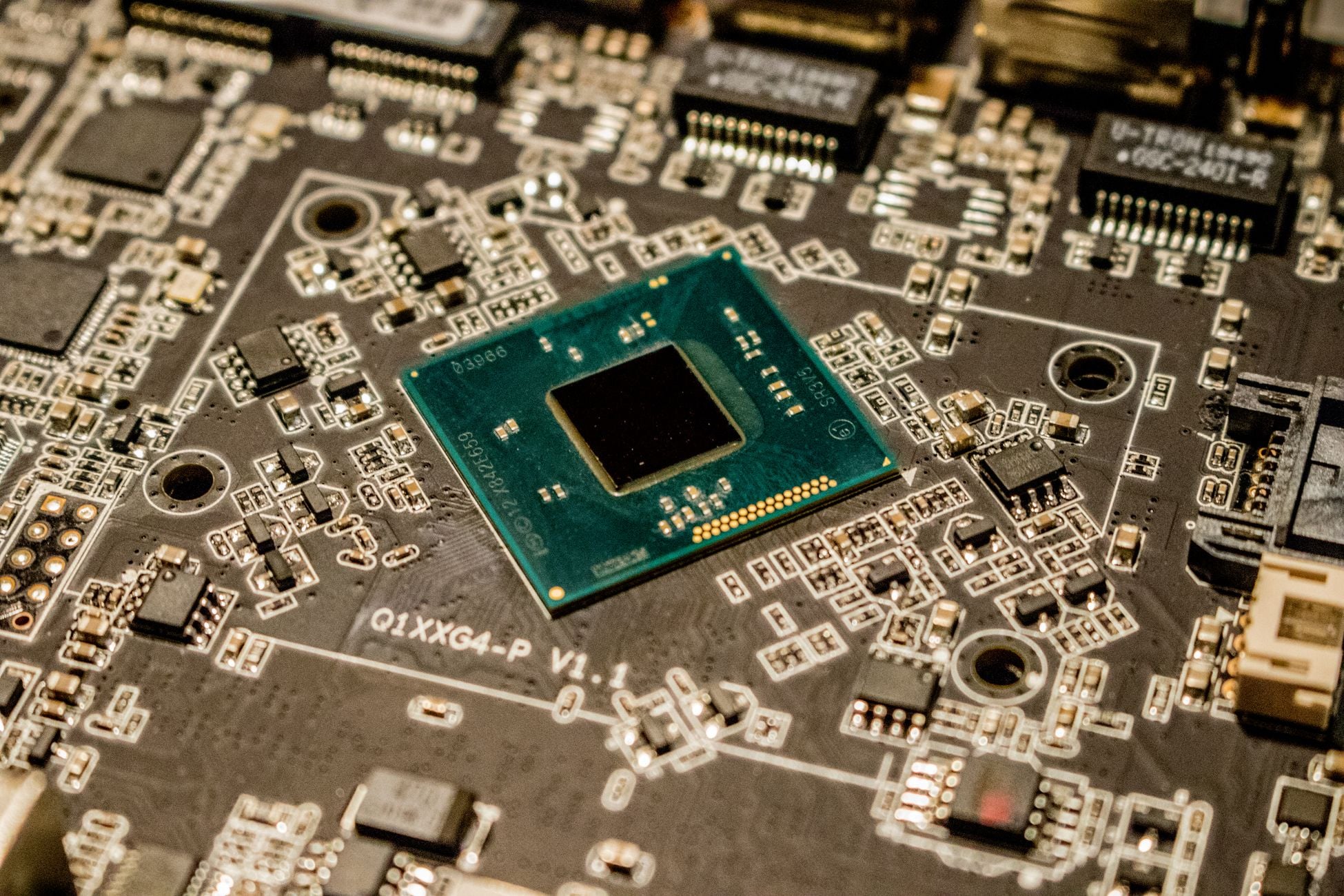
Inside TSMC’s Fab 18 complex in Tainan, Taiwan, ultraviolet light with a wavelength of 13.5 nanometers, generated by vaporising tin droplets with a laser 50,000 times a second, etches transistor patterns smaller than a strand of DNA onto 300-millimeter silicon wafers. The chips coming off those lines, built on what the industry calls 7-nanometer and more advanced nodes, accounted for 74% of Taiwan Semiconductor Manufacturing Company’s wafer revenue in 2025. The frontier of computing, the part of the supply chain that almost no other company on Earth can do at scale, has quietly become nearly the entire business of a single firm in a single country.
It is a stunning concentration. Ten years ago, the same category, 7nm and beyond, was zero percent of TSMC’s revenue, because nobody made chips that small yet.
What “7 nanometers and beyond” actually means
The node names are partly marketing. A “3-nanometer” transistor does not have any feature that is literally three nanometers across. The numbers are a shorthand for a generation of process technology, each one denser, faster, and more power-efficient than the last.
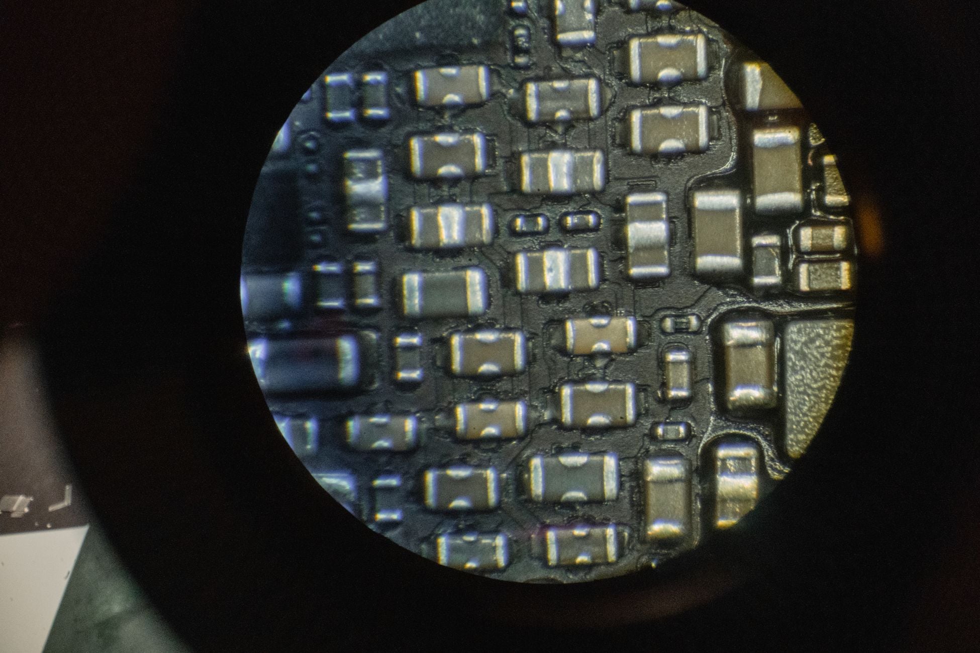
What is real is the size of the transistors themselves. On TSMC’s N3 process, the transistor density runs to roughly 200 million transistors per square millimeter. An Apple M3 chip, fabricated on that node, packs about 25 billion transistors into a piece of silicon smaller than a postage stamp. The wires connecting them are narrower than the smallest viruses.
Building anything at that scale requires extreme ultraviolet lithography machines made by a single Dutch company, ASML. Each one costs around $200 million and weighs roughly 180 tonnes, shipped to customers in dozens of specialised containers across multiple Boeing 747s. TSMC owns more of them than anyone else.
The 74% number, in context
TSMC reports its wafer revenue by process node every quarter. In 2015, the company’s most advanced offering was 16nm, and it made up a small fraction of sales. The bulk of revenue came from older nodes. 28nm, 40nm, 65nm. Chips used in everything from car dashboards to washing-machine controllers.
By 2020, 7nm alone was about a third of revenue. By 2025, the combined share of 7nm, 5nm, and 3nm reached that 74% figure. The mature nodes that used to be the company’s bread and butter still exist, still earn money, but they are now a minority of the wafer business.
The shift maps almost perfectly onto the rise of two things: the smartphone application processor and, more recently, the AI accelerator. Apple’s A-series and M-series silicon, Nvidia’s H100 and Blackwell GPUs, AMD’s MI300 series, and Google’s Tensor Processing Units are all fabricated by TSMC on its leading-edge lines.
Why nobody else can do this
Three companies in the world can build chips at 7nm or below: TSMC, Samsung Foundry, and Intel. Of those three, TSMC has dominant yield and the deepest customer book by a wide margin. At 3nm and 2nm, the company’s lead is more pronounced. Intel is still climbing back into the race with its 18A process, and Samsung has been losing major customers.
In May 2026, AMD announced it would split some of its 2nm orders to Samsung, a small dent in TSMC’s near-monopoly on bleeding-edge AI silicon. The decision was driven less by Samsung’s technical parity than by AMD’s desire not to have all of its inventory exposed to a single supplier in a single geography.
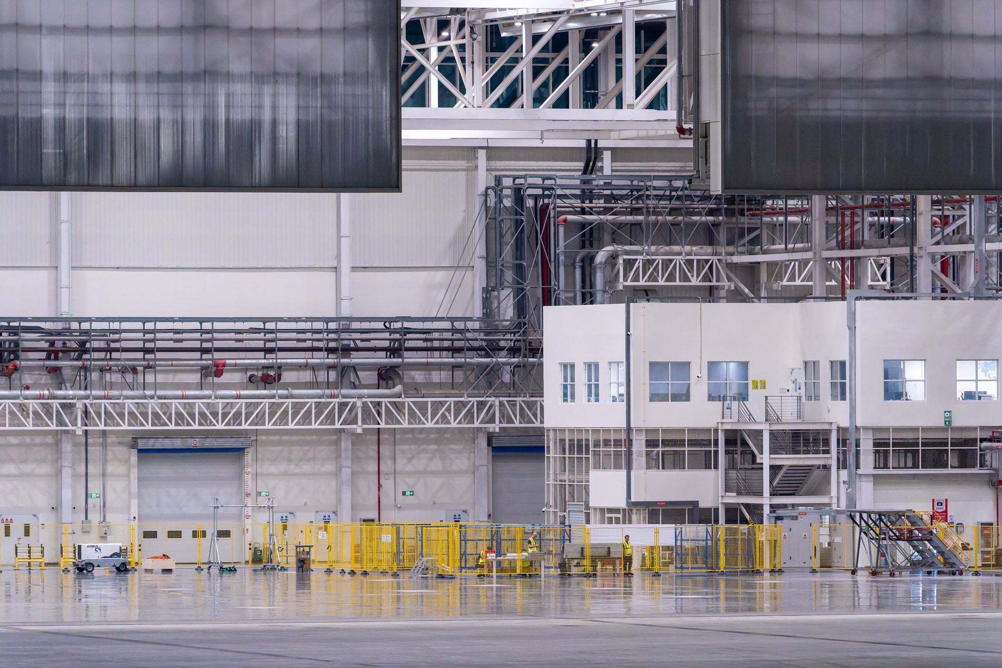
That geography is the crux of the matter. The vast majority of TSMC’s most advanced fabs sit on a narrow strip of western Taiwan, about 100 miles long, in the Hsinchu, Taichung, and Tainan science parks. The island is one of the most seismically active places on the planet and sits in a contested strait.
The customers TSMC has, and what they make
Apple is TSMC’s largest customer and has been for over a decade. Every iPhone processor since the A10 in 2016 has been manufactured exclusively in Taiwan, with TSMC also fabricating the earlier A8 in 2014 and a share of the dual-sourced A9. Nvidia, whose H100 and B200 chips power most of the world’s generative AI training clusters, is the second-largest. AMD, Qualcomm, Broadcom, and MediaTek round out the top tier.
The dependency runs the other way too. TSMC’s own forecast puts the 2030 chip market at $1.5 trillion, with 55% of demand tied to AI and high-performance computing. The company expects to capture a disproportionate share of that growth because the chips driving it, large transformer accelerators, custom ASICs, advanced CPUs, all require nodes only it can produce in volume.
Every ChatGPT response, every Midjourney render, every Gemini query touches silicon that left a Tainan cleanroom.
Why the share keeps climbing
Older nodes are getting commoditised. Chinese foundries like SMIC and HuaHong have built substantial 28nm and 14nm capacity, and they sell into the automotive, industrial, and consumer markets at prices TSMC has little interest in matching. The mature-node business is becoming a margin-thin commodity game.
Meanwhile, the leading edge is becoming more expensive and more profitable. A single 3nm wafer reportedly sells for around $20,000, compared to roughly $3,000 for a 28nm wafer a decade ago. The chips that come off it are denser and more valuable. The customers paying for them. Apple, Nvidia, AMD. They have the gross margins to absorb the price.
So TSMC’s revenue mix tilts toward the frontier not just because the frontier is growing, but because the rest is being eaten from below.
The Arizona experiment
To diversify the geographic risk, TSMC has been building fabs outside Taiwan. The Phoenix, Arizona site began limited production of 4nm chips in late 2024, and the second and third Arizona fabs are planned for 3nm and 2nm. Construction is also underway in Kumamoto, Japan, and Dresden, Germany.
None of these match the scale or sophistication of the Taiwan operations. The Arizona fabs are expected to produce a small fraction of TSMC’s leading-edge output by 2030. Workforce, supply chain, and ecosystem effects make the home island difficult to replicate.
Nvidia’s own Taiwan investment, announced by Jensen Huang in May 2026, signalled a new AI supply chain reality: the most ambitious AI companies are doubling down on the island even as governments push for diversification.
The cost of staying ahead
Each new node costs more to develop than the last. TSMC’s capital expenditure for 2025 ran north of $40 billion, most of it on EUV machines, building shells, and the specialised tooling for 2nm production. The 2nm node, branded N2, entered volume production in late 2025 and will ramp through 2026.
Below 2nm, the industry has to abandon FinFET transistors for a new architecture called gate-all-around, which TSMC calls Nanosheet. The first such chips will use transistors so small that quantum tunneling, electrons leaking through walls that are too thin to contain them, becomes a major engineering problem.
Analysts tracking TSMC’s growth trajectory toward 2030 have noted that the company’s stock could triple over the next five years if AI demand continues to scale alongside the leading-edge mix.
What 74% means for the rest of the world
If TSMC’s leading-edge production were to stop tomorrow, through earthquake, blockade, or accident, there would be no meaningful substitute for at least three years. Samsung could absorb some volume at 5nm and 3nm but not at the yields Apple and Nvidia need. Intel’s 18A is unproven at scale. SMIC in China has been stuck at 7nm-equivalent under U.S. export controls.
The consequence would not be a temporary shortage. It would be a multi-year pause in the rollout of new iPhones, new AI accelerators, new gaming GPUs, new server CPUs. Existing inventory would last months, not years. Even peripheral suppliers in the AI chip ecosystem are working to reduce single-customer, single-geography exposure as a hedge against this scenario.
The transistor that does not really exist
In the Tainan fabs at this moment, machines are stacking layers of silicon, hafnium, and tungsten one atom at a time onto wafers that will become the brains of the next generation of phones and AI servers. Each transistor on a 2nm chip is roughly the width of ten silicon atoms laid side by side. There are about 100 billion of them on a single processor.
That 74% figure, a corporate revenue mix from a quarterly report, is shorthand for something stranger. The frontier of human manufacturing, the most precise industrial process ever achieved, has narrowed to a handful of cleanrooms on one island, run by one company, fed by one Dutch supplier of light sources. Everything downstream of it. The consumer electronics industry, the cloud computing industry, the AI industry. All of it sits on top of that single point.
The light flickers 50,000 times a second. The wafers keep moving.